- 您现在的位置:买卖IC网 > Sheet目录310 > AL8400SE-7 (Diodes Inc)IC CTRLR LED DRIVER SOT353
�� �
�
�AL8400� /AL8400Q�
�Application� Information� (cont.)�
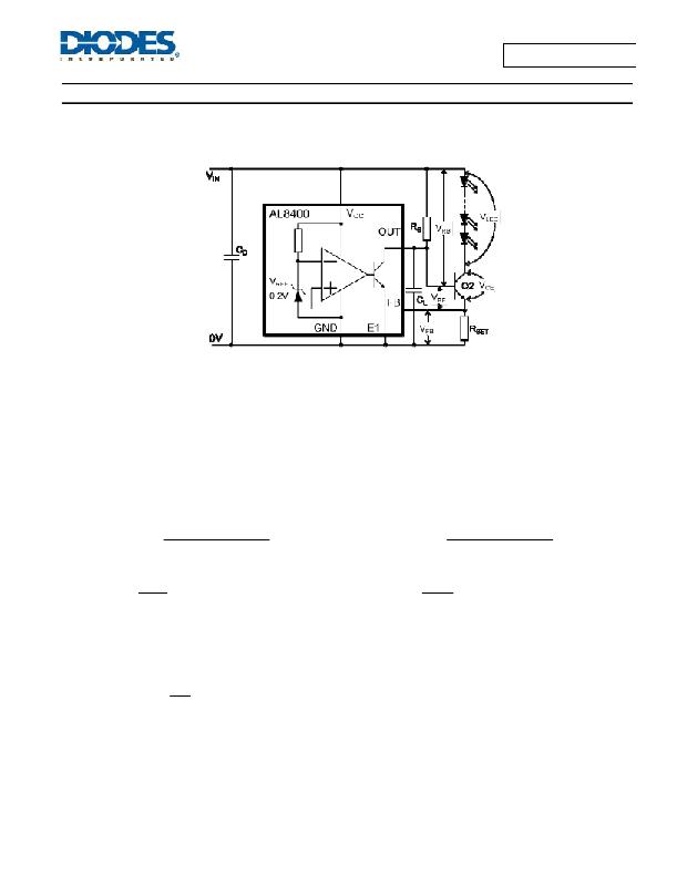
�Bipolar� Transistor� as� the� Pass� Element�
�For� driving� currents� in� the� region� of� about� 50mA� to� about� 400mA,� the� recommended� NPN� is� DNLS320E� in� the� SOT223� package.� The� high� DC�
�current� gain� of� the� DNLS320E� is� useful� in� this� application,� in� order� to� minimize� the� current� in� R� B� .� The� design� procedure� is� as� follows,� referring� to�
�Figure� 4.�
�Figure� 4� Application� Circuit� Using� Bipolar� Transistor�
�There� are� two� important� equations� for� the� circuit:�
�LED� Circuit� Path:�
�1.�
�V� CC� =� (V� LED� +� V� CE� +� V� FB� )� where� V� FB� is� approximately� the� internal� reference� voltage� of� 200mV.�
�The� maximum� total� LED� voltage� plus� the� reference� voltage� determines� the� minimum� supply� voltage.� Substituting� into� equation� 1� yields:�
�V� CC� min� =� V� LED� max� +� V� CEsat� +� V� FB� where� V� LEDmax� is� the� maximum� LED� chain� voltage.�
�Control� Drive� Circuit� Path�
�2.�
�V� CC� =� (V� RB� +� V� BE� +� V� FB� )�
�For� a� bipolar� transistor� the� voltage� (V� RB� )� across� bias� resistor� R� B� consists� of� the� base� current� of� Q2� and� the� output� current� of� the� AL8400.� So�
�rearranging� equation� 2� yields� the� boundaries� for� allowable� R� B� values:�
�3.�
�R� B� max� =�
�V� CC min� ?� V� BE max� ?� V� FB�
�I� OUT� min� +� I� B� max�
�4.�
�R� B� min� =�
�V� CC max� ?� V� BE min� ?� V� FB�
�I� OUT� max� +� I� B� min�
�where� I� Bmax� is� the� maximum� transistor� base� current�
�where� I� Bmin� is� the� minimum� transistor� base� current�
�I� B� max� =�
�I� LED�
�h� FE� min�
�I� B� min� =�
�I� LED�
�h� FE� max�
�where� h� FEmin� is� the� minimum� DC� current� gain� of� the� transistor.�
�where� h� FEmax� is� the� maximum� DC� current� gain� of� the� transistor.�
�The� value� of� R� B� should� be� set� somewhere� between� R� Bmax� and� R� Bmin� with� the� target� of� trying� to� get� I� OUT� of� the� AL8400� close� to� 1mA� for� nominal�
�conditions.�
�Once� R� B� has� been� determined� the� value� for� compensation� capacitor,� C� L� ,� should� be� calculated.�
�C� L� ≈�
�2ms�
�R� B�
�Finally,� the� bipolar� selection� is� also� influenced� by� the� maximum� power� dissipation�
�P� TOT� =� I� LED� x� (V� CC� –� V� LED� –� V� REF� )� =� I� LED� x� V� CE�
�Since� this� determines� the� package� choice� (� θ� JA� )� in� order� to� keep� the� junction� temperature� below� the� maximum� value� allowed.�
�T� J� =� T� A� +� P� TOT� x� θ� JA�
�where�
�T� J(MAX)� is� the� maximum� operating� junction� temperature,�
�T� A� is� the� ambient� temperature,�
�θ� JA� is� the� junction� to� ambient� thermal� resistance.�
�AL8400/� AL8400Q�
�Document� number:� DS35115� Rev.� 4� -� 2�
�6� of� 13�
�www.diodes.com�
�August� 2012�
�?� Diodes� Incorporated�
�发布紧急采购,3分钟左右您将得到回复。
相关PDF资料
AL8805W5-7
IC REG SW CONV BUCK ASYNC SOT-23
AL8806MP8-13
IC LED DVR CONS CURR 8MSOP
AL8807W5-7
IC LED DRVR DCDC BUCK SOT25
AL9910AS-13
IC LED DRVR HIGH BRIGHT SO8EP
ALC60481R05
PWR SUP AC-DC 6-48V 1.05A 50.4W
ALV100362R5
POWER SUPPLY AC-DC 36V 2.5A 90W
ALV60361R7
POWER SUPPLY AC-DC 36V 1.7A 61W
ALV80126R5
POWER SUPPLY AC-DC 12V 6.5A 78W
相关代理商/技术参数
AL841B
制造商:ELC 功能描述:PSU BENCH MULTI OUTPUT 制造商:ELC 功能描述:PSU, BENCH, MULTI OUTPUT, EURO
AL8504
制造商:Molex 功能描述:
AL-85-120VAC
制造商:Carlo Gavazzi 功能描述:LATCH UNIT 50-85A
AL875
制造商:未知厂家 制造商全称:未知厂家 功能描述:Triple High Speed, 8-bit Analog-to-Digital Converter
AL8805
制造商:DIODES 制造商全称:Diodes Incorporated 功能描述:HIGH EFFICIENCY 30V 1A BUCK LED DRIVER
AL8805EV1
功能描述:AL8805 1, Non-Isolated Output LED Driver Evaluation Board 制造商:diodes incorporated 系列:- 零件状态:有效 电流 - 输出/通道:680mA 输出和类型:1,非隔离 电压 - 输出:- 特性:可调光 电压 - 输入:6 V ~ 36 V 所含物品:板 使用的 IC/零件:AL8805 标准包装:1
AL8805EV2
功能描述:AL8805 1, Non-Isolated Output LED Driver Evaluation Board 制造商:diodes incorporated 系列:- 零件状态:有效 电流 - 输出/通道:680mA 输出和类型:1,非隔离 电压 - 输出:- 特性:- 电压 - 输入:12VAC,12 V ~ 20 V 所含物品:板 使用的 IC/零件:AL8805 标准包装:1
AL8805W5-7
功能描述:LED照明驱动器 HI EFF 30V 1A BUCK LED DRIVER RoHS:否 制造商:STMicroelectronics 输入电压:11.5 V to 23 V 工作频率: 最大电源电流:1.7 mA 输出电流: 最大工作温度: 安装风格:SMD/SMT 封装 / 箱体:SO-16N